
|
|
|
|
|
|
|
|
|
|||||||
|
||||||||
|
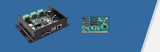
Product
Tools, Drivers, etc |
GESBC-9G25iProduct SupportPre-compiled Binary Images Pre-compiled boot strap code. Pre-compiled device tree binary. Pre-compiled Linux 4.5.2 kernel image. Embedded Linux file system UBI image Embedded Linux File System. Pre-compiled boot strap code. Pre-compiled device tree binary. Pre-compiled Linux 4.5.2 kernel image. Embedded Linux file system UBI image Embedded Linux File System.
Board Connection Diagram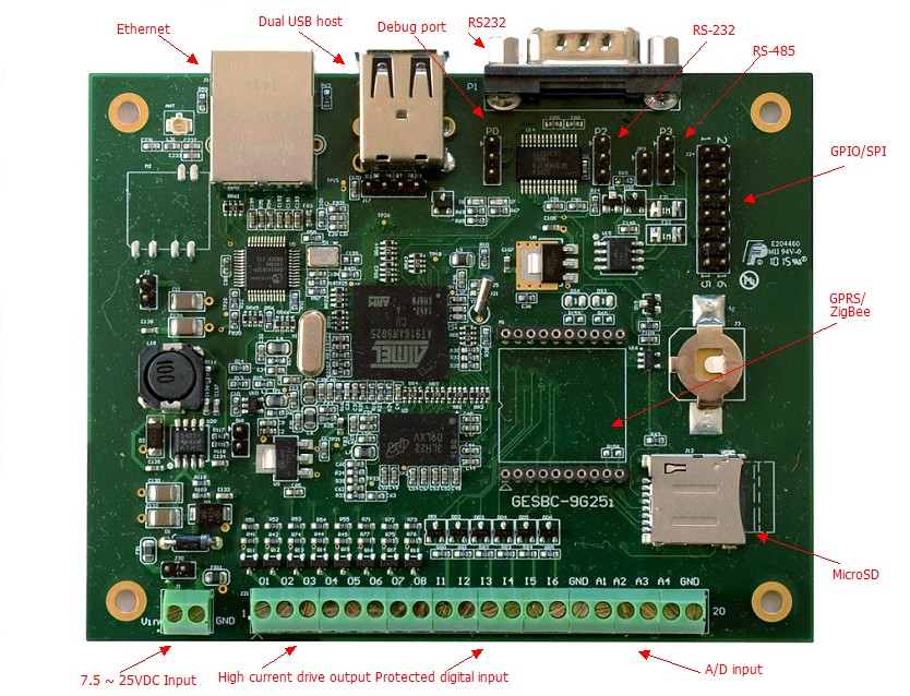
Getting StartedThe GESBC-9G25i comes from factory with Linux pre-installed and ready to run.
When GESBC-9G25i powers up the system boot message will be displayed on the terminal screen.
Power ConnectionThe GESBC-9G25i Industrial Computer can use a wide range of DC power supply.
JTAG ConnectionThe GESBC-9G25i supports JTAG interface. The JTAG connection is on the back side of the PCB with a 2x5 surface mount header (unpopulated from factory). The JTAG signal arrangement is shown in the following table
RS-232 Port connectionThe GESBC-9G25i has a debug serial port P0 that can be connected to desktop system to debug/monitor system. The debug serial port communication settings are 115200,8,N,1. The DB9 connector P1 on the GESBC-9G25i connects to USART2 of the processor. The header connector P2 is connected to the UART0 of the processor.
RS-485 ConnectionThe RS-485 interface on the GESBC-9G25i is on the 3 pin 2.54mm spacing header P3. It is connected to USART0 of the AT91SAM9G25 processor. The Linux device node is /dev/ttyS1.
Sample RS-485 communication C program to send data through the RS-485 port.
ZigBee NetworkZigBee is a wireless technology developed as an open global standard to address the unique needs of low-cost, low-power wireless M2M networks. Applications include wireless light switches, electrical meters with in-home-displays, traffic management systems, and other consumer and industrial equipment. The GESBC-9G25i contains a socket to provide direct plug-in interface to XBee line of modules by Digi. The GESBC-9G25i can be easily configured as ZigBee network gateway with the ZigBee plug-in module. The XBee socket M1 signals are listed in the following table,
The serial port connected to the XBee socket is USART3, which corresponds to /dev/ttyS4 in Linux. Note: pins not listed in the above table have no connection on the GESBC-9G25i.
High Current Digital Output PortsThe GESBC-9G25i has 8 high current drive digital outputs. The driver stage uses power MOSFET. The maximum voltage is 60VDC. The maximum continuous drain current @10VDC @32° is 1.2A. The terminal block J21 provides the digital output connection.
The output port can be controlled by sending a logic 1 or 0 to the corresponding device node. For example, echo "1" > /sys/class/gpio/pioC10/value Please note a logic value 1 send to the output will turn on the output MOSFET and pull the output low.
Protected Digital InputsThe GESBC-9G25i has 6 protected digital inputs. The protected inputs can withstand over voltage up to 30V.
The input value can be read directly from the device node, for example, cat /sys/class/gpio/pioA26/value
4 channel 10 bit analog inputsThe GESBC-9G25i has 4 channel single ended analog inputs connected to the on-chip A/D.
Digital GPIO (LVTTL)/IO ExpansionThe GESBC-9G25i has 14 LVTTL digital GPIO lines on J24 that also includes SPI and I2C bus. These GPIO ports are connected directly to the ARM processor. The maximum output current is 4mA.
FLASH memory Allocation Map From FactoryThe GESBC-9G25i has 128MB of NAND FLASH. The FLASH memory is "soft" partitioned into several regions as system storage. The storage map is shown in the following table.
The kernel image is configured to have 'Use appended device tree blob to zImage' option. The device tree binary must be appended using the following command, # cat <dtb_file_name> >> zImage
Update System SoftwareThe Linux kernel and device tree binary can be updated in-system. The following example updates the Linux kernel image in the NAND FLASH, # flash_eraseall /dev/mtd2 # nandwrite -p /dev/mtd2 zImage Please note the example above assumes the kernel image size is less than 6MByte. The NAND FLASH must be erased before writing new kernel image.
Application DevelopmentCross DevelopmentA Linux based host system can be used as the cross development system. To use a general purpose Linux desktop for cross development the ARM Linux cross compiler and commonly used development tools must be installed. The factory installed embedded file system is based on Buildroot 2015.02 using glibc 2.19, binutils 2.25. The cross compiler tool chain must have compatible library in order for the cross compiled program to run on the target system. Below is a simple example cross compiling the hellowWorld application, arm-linux-gnueabi-gcc -o helloWorld helloWorld.c With cross compiler tool chain and development tools properly installed the cross compiling process is no different than native compiling process except the compiler name would be the cross compiler name. Below are two pre-built Linux virtual machine images (compatible with VMWare VMWorkstation VMPlayer) has ARM cross development tools installed and ready to use.
In-System DevelopmentThe GESBC-9G25i also supports on-target development that allows developer to write, compile, and test program on-target. The following easy step-by-step instructions demonstrates the simple process,
          # mkfs.ext2 /dev/sda1
                  or
          # mkfs.ext2 /dev/mmcblk0p1
          # mount /dev/sda1 /mnt
                  or
          # mount /dev/mmcblk0p1 /mnt
          # cd /mnt
          # wget http://www.glomationinc.com/Support/GESBC-9G25w/debian-armel-8.4.xz
          # tar xf debian-armel-8.4.xz
# mkdir -p /mnt/proc
          #apt-get install gcc
          ...
The above steps only need to be done once to prepare the USB/SD storage. To switch to the on-target development system, # mount /dev/sda1 /mnt (if it has not been mounted)
# mount -t proc proc /mnt/proc
# chroot /mnt /bin/sh
Use the exit command to leave the development environment. Please remember to umount the /mnt/proc after leaving the development environment. # umount /mnt/proc
Additional InformationFor customers that would like to build their own Linux kernel and/or file system. The following link provides information on build tools, kernel source, etc. Linux & Open Source related information for Atmel AT91SAM9Gx5 ARM Microcontrollers |